La tecnología moderna de semiconductores opera a una escala sin precedentes. A medida que los nodos de circuito se reducen al nivel nanométrico, los circuitos integrados (CI) se vuelven exponencialmente más vulnerables a los eventos de descarga electrostática (ESD). Incluso una descarga menor de menos de 100 voltios puede causar fallas catastróficas en estos delicados microchips. En consecuencia, los materiales utilizados para las bandejas de transporte, los portadores de obleas y las carcasas de componentes desempeñan un papel fundamental en la confiabilidad de la fabricación. Los equipos de ingeniería a menudo debaten la necesidad de materiales protectores especializados frente a polímeros estándar. Los datos de la industria sugieren que el cambio haciaLámina ABS ESD personalizada Ha pasado de ser un lujo a un requisito básico para el empaquetado de semiconductores de alto rendimiento. Este análisis evalúa la divergencia técnica entre el acrilonitrilo butadieno estireno (ABS) estándar y las variantes conductoras diseñadas, centrándose en cómo estas elecciones de materiales influyen en la seguridad a largo plazo de los dispositivos.
P1: ¿En qué se diferencian la resistividad superficial y la cinética de decaimiento de carga entre las láminas de ABS estándar y las láminas de ABS ESD personalizadas?
La principal diferencia entre los polímeros estándar y los conductores radica en su comportamiento eléctrico. El ABS estándar funciona como un aislante eléctrico de alta calidad, con una resistividad superficial que suele superar los 10¹² ohmios por cuadrado. Si bien esta propiedad aislante impide la entrada de corriente externa, crea un entorno peligroso para los componentes sensibles a la estática. La fricción durante la manipulación genera cargas triboeléctricas que se acumulan en la superficie del ABS aislante. Debido a que el material inhibe el movimiento de carga, estos electrones atrapados permanecen hasta que un objeto, como una placa de circuito impreso o un dedo, proporciona una vía a tierra. Esta liberación repentina de energía almacenada produce una descarga electrostática (ESD) que puede destruir los microcircuitos.
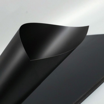
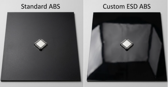
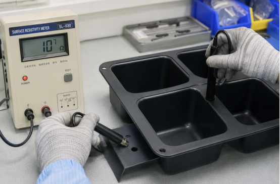
En contraste, las láminas de ABS ESD personalizadas incorporan rellenos conductores, generalmente negro de humo, para crear una red interna estable. Esta modificación reduce la resistividad superficial a un rango de entre 10⁶ y 10⁹ ohmios por cuadrado. Este rango proporciona el equilibrio perfecto para el control de la estática, permitiendo que el material disipe las cargas de forma segura a tierra sin provocar un cortocircuito. Además, la cinética de decaimiento de la carga demuestra este control superior. Mientras que el ABS estándar retiene cargas estáticas durante períodos prolongados, los materiales con grado ESD pueden disipar una carga de 5000 voltios hasta casi cero en menos de dos segundos. Esta rápida tasa de decaimiento elimina la acumulación de electricidad estática, protegiendo eficazmente los chips semiconductores de una posible ruptura dieléctrica.
P2: ¿Qué ocurre con la barrera protectora durante el termoformado intenso? Comparación de la distribución del espesor y la estabilidad de la impedancia.
El termoformado sigue siendo el proceso más común para crear portadores semiconductores complejos. Sin embargo, este proceso genera una tensión considerable en el material. Cuando los fabricantes introducen una lámina de plástico caliente en un molde profundo, el material se estira y se adelgaza en ciertas zonas. El ABS estándar generalmente mantiene su resistividad durante este proceso de adelgazamiento, ya que sus propiedades aislantes dependen de la cadena polimérica base, no de una red de aditivos.
Por el contrario, los materiales con protección ESD presentan un complejo desafío de ingeniería durante el termoformado. Si la red conductora se rompe durante la fase de estiramiento, el material desarrolla puntos calientes donde la resistividad aumenta significativamente, lo que inutiliza la bandeja. Por lo tanto, la calidad de la dispersión del relleno conductor determina el éxito de la pieza. La fabricación de alto rendimiento utiliza técnicas de composición sofisticadas para garantizar que las vías conductoras permanezcan interconectadas incluso después de que el material se estire hasta un 300 % de su tamaño original.
Xiamen Fullstar Imp.&Exp.Trading Co.,Ltd. aborda este desafío empleando tecnología de negro de humo de alta dispersión. Este enfoque garantiza que la impedancia permanezca uniforme en toda la superficie de la bandeja, independientemente de la relación de embutición. Cuando los ingenieros comparan la resistividad de la sección transversal de una bandeja de embutición profunda, los materiales personalizados superan sistemáticamente a las variantes estándar al mantener características eléctricas estables. Esta estabilidad evita las fallas impredecibles que a menudo se asocian con materiales de menor calidad.Láminas de plástico ABS negro ESD al por mayordonde la red conductora podría ser demasiado escasa para soportar la tensión mecánica del moldeo.
P3: Más allá de los rellenos conductores, ¿cómo mejora aún más la protección una estructura compuesta de ABS/TPU durante el conformado por embutición profunda?
La dispersión del relleno conductor no es la única variable que determina si una bandeja sobrevive intacta al termoformado por embutición profunda. El sustrato base en sí mismo desempeña un papel igualmente importante. El ABS ESD monocapa estándar, si bien es eléctricamente eficaz, puede desarrollar microfisuras en las esquinas afiladas de las cavidades y en las líneas de pliegue cuando se estira para formar geometrías complejas, un punto de fallo común en los portaobleas y las bandejas de componentes multicavidad.
Para solucionar este problema, los fabricantes más avanzados laminan la capa conductora de ABS con una fina capa de TPU (poliuretano termoplástico), creando una lámina compuesta que conserva la rigidez y la estabilidad dimensional necesarias para el soporte estructural, a la vez que adquiere la flexibilidad y elasticidad del TPU en los puntos de tensión. Esta construcción de ABS/TPU absorbe los impactos mecánicos durante la manipulación y reduce el riesgo de agrietamiento o deslaminación en las esquinas de embutición profunda, lo que prolonga la vida útil de las bandejas en los ciclos repetidos de uso y devolución habituales en la logística de semiconductores.
La estructura compuesta amplía el ámbito de aplicación más allá de las bandejas rígidas de un solo material. Gracias a que la capa de TPU proporciona amortiguación sin comprometer la resistencia superficial ESD de la capa de ABS, la misma lámina se puede termoformar para crear diseños de cavidades más profundas y complejas, como bandejas de matriz, soportes de conectores y revestimientos amortiguadores para componentes de forma irregular, sin comprometer el control de la estática. Las láminas compuestas de ABS/TPU de Fullstar están diseñadas específicamente para este doble requisito, admitiendo espesores de 0,3 mm a 3,0 mm y anchos de hasta 950 mm, y siendo totalmente reciclables para contribuir a los objetivos de sostenibilidad de los clientes.
Q4: ¿Por qué la contaminación por partículas y "c¿El desprendimiento de carbono hace que los materiales estándar queden obsoletos en entornos de salas blancas?
La industria de los semiconductores mantiene estándares rigurosos para salas blancas, que a menudo requieren entornos de Clase 10 o Clase 100. En estos espacios controlados, incluso una partícula de polvo microscópica puede crear un puente entre los contactos eléctricos y dañar una oblea de silicio. Esta realidad pone de manifiesto el segundo gran defecto del ABS aislante estándar: su tendencia a atraer polvo. Dado que el ABS estándar actúa como un imán estático, atrae las partículas suspendidas en el aire hacia su superficie mediante atracción electrostática. Una vez contaminadas, estas bandejas introducen residuos extraños en el ciclo de empaquetado, creando un riesgo oculto difícil de detectar.
Sin embargo, la industria se enfrenta a un problema igualmente peligroso con los materiales ESD mal fabricados: el desprendimiento de carbono. Si los rellenos conductores no están correctamente encapsulados dentro de la matriz de ABS, pueden desprenderse de la superficie en forma de polvo fino. Este fenómeno sustituye la electricidad estática por contaminación física. En la fabricación de alto riesgo, el polvo de carbono conductor es tan peligroso como la electricidad estática, ya que puede provocar cortocircuitos en los terminales sensibles de los chips.
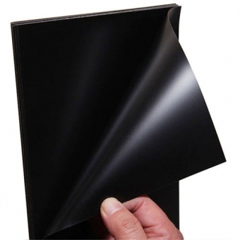
Para solucionar este problema se requiere una fabricación de precisión. Fullstar utiliza una aleación patentada que fija las partículas conductoras de forma segura dentro de la estructura del polímero. Este proceso de fabricación especializado garantiza que la superficie negra de alto brillo se mantenga lisa y sin desprendimiento de partículas. Al lograr este equilibrio, el material proporciona la disipación eléctrica necesaria sin comprometer la pureza física exigida por los estándares de las salas blancas. Una comparación objetiva demuestra que las láminas de ABS modernas, formuladas a medida, eliminan el desprendimiento de partículas que afectaba a las primeras versiones de plásticos conductores.
Q5Desde dimensiones personalizadas hasta muestreo rápido, ¿cómo influye la adaptabilidad de la fabricación en el riesgo de las compras B2B globales?
Seleccionar el material adecuado es solo el primer paso en el proceso de adquisición. Los responsables de la cadena de suministro global también deben evaluar la adaptabilidad técnica del socio fabricante. La industria de los semiconductores avanza a un ritmo vertiginoso, lo que exige un embalaje que cumpla con las especificaciones exactas de tamaño de oblea, altura de componente y alineación del cargador. Un proveedor que solo ofrece láminas estándar disponibles en el mercado suele obligar a los responsables de compras a sacrificar la eficiencia del diseño.
La adaptabilidad en la fabricación abarca varias dimensiones, incluyendo la capacidad de controlar el espesor del calibre desde tan solo 0,2 mm hasta 3,0 mm, y la capacidad de proporcionar cortes de ancho precisos.Fullstar (Xiamen Fullstar Imp.&Exp.Trading Co.,Ltd.) Mitiga estos riesgos mediante la integración de capacidades de producción integrales. Con tres bases de producción especializadas y tecnología de coextrusión multilínea, la empresa gestiona tanto la producción a gran escala como la creación rápida de prototipos en lotes pequeños.
Al salvar la brecha entre la ciencia de las materias primas y los requisitos de termoformado a medida, el fabricante reduce el tiempo de comercialización de nuevos productos semiconductores. Una evaluación objetiva de la cadena de suministro demuestra que las fábricas capaces de proporcionar certificaciones técnicas detalladas, como registros de resistividad superficial e informes de espesor, ofrecen un valor superior. Los equipos de compras que optan por estos socios evitan los problemas comunes de la calidad inconsistente de los materiales y los plazos de envío impredecibles.
Aplicaciones típicas de láminas compuestas de ABS/ABS-TPU ESD personalizadas
· Bandejas portaobleas y bandejas de matriz de circuitos integrados para fábricas de semiconductores.
· Bandejas de transporte y almacenamiento de PCB/PCBA para líneas de producción SMT
· Bandejas blíster de embutición profunda para conectores, sensores y componentes de precisión.
· Revestimientos protectores antiarañazos y libres de polvo para el montaje de componentes electrónicos en salas blancas.
· Embalaje amortiguador y revestimientos protectores industriales para piezas irregulares o frágiles.
· Embalaje para exportación y logística de módulos electrónicos sensibles a la estática
Conclusión: Lecciones estratégicas y el futuro del empaquetado de semiconductores
La evidencia favorece claramente las láminas de ABS ESD personalizadas para aplicaciones modernas de empaquetado de semiconductores. Si bien el ABS estándar cumple su función en entornos no sensibles, no proporciona el control eléctrico crítico necesario para los microchips de alta densidad actuales. Al elegir materiales conductores diseñados a medida, los fabricantes garantizan un entorno fiable, estable y limpio que preserva directamente el valor de sus componentes. Esta selección reduce las tasas de defectos latentes, simplifica el mantenimiento de la sala limpia y optimiza la fiabilidad estructural de todo el sistema de empaquetado. Para los equipos de ingeniería y compras encargados de asegurar la próxima generación de electrónica de semiconductores, es esencial centrarse en la selección de materiales de alto rendimiento. Obtenga más información sobre soluciones profesionales de materiales ESD enhttps://www.fullstarxm.com/.
XIAMEN FULLSTAR IMP.& EXP. TRADING CO.,LTD.


 red ipv6 compatible
 escanear a wechat :

 fullstar@xmfullstar.com
 es
es en
en ru
ru