Las líneas de envasado electrónico automatizadas en 2026 operan a velocidades extremadamente altas y con márgenes de beneficio estrechos. Los fabricantes de productos electrónicos deben envasar componentes delicados como microchips, circuitos integrados y sensores de forma segura. Cualquier defecto mecánico en la cinta portadora o en la bandeja puede provocar que las líneas automatizadas se atasquen, lo que genera costosos tiempos de inactividad. Además, las grietas físicas o las rebabas de plástico generadas durante el troquelado pueden contaminar los componentes sensibles. Mientras que los gerentes de envasado de alimentos podrían buscar un proveedor de láminas de PP de grado alimenticio certificado para garantizar la pureza química, los ingenieros de envasado electrónico requieren Soluciones de láminas de HIPS para termoformado OEM/ODM para minimizar los gastos generales de fabricación. Los materiales poliméricos estándar y disponibles en el mercado a menudo no cumplen con las rigurosas exigencias de las modernas líneas de ensamblaje automatizadas. Cuando las láminas de plástico no resisten las altas velocidades de troquelado, se forman microfisuras alrededor de los bordes cortados. Estas pequeñas fracturas pueden extenderse, provocando que toda la bandeja falle durante el transporte. Además, la clasificación manual de los envases defectuosos aumenta drásticamente los costos laborales y ralentiza los cronogramas de entrega. Para seguir siendo competitivos, los envasadores de productos electrónicos deben encontrar formas de reducir este desperdicio mecánico. Deben optimizar sus materiales para garantizar un funcionamiento fluido y el máximo rendimiento en líneas de alta velocidad. En última instancia, la reducción de costos depende de la elección de materiales diseñados específicamente para las tensiones físicas únicas de la maquinaria de envasado automatizada. Al centrarse en propiedades poliméricas personalizadas, los fabricantes pueden evitar fallos mecánicos antes de que afecten a los resultados finales. Los dispositivos electrónicos modernos requieren un alto grado de protección física.
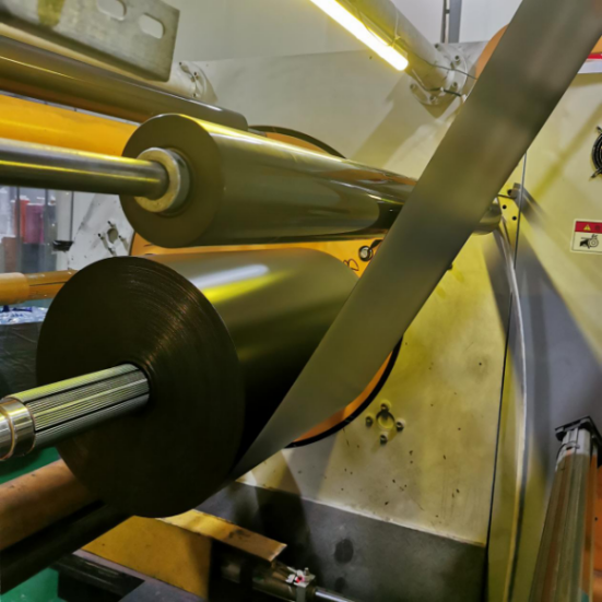
El poliestireno de alto impacto, o HIPS, es un material popular para el envasado de productos electrónicos debido a su perfil mecánico único. La matriz polimérica consiste en una fase rígida de poliestireno mezclada con una fase flexible de caucho de polibutadieno. Esta dispersión de elastómero le da al HIPS su característica resistencia al impacto, permitiéndole absorber energía mecánica. Sin embargo, la proporción y el tamaño de partícula de la fase de caucho deben coincidir con las demandas precisas del troquelado de alta velocidad. Si el contenido de caucho es demasiado bajo, la lámina se vuelve quebradiza y propensa a agrietarse bajo la presión del punzón. Por el contrario, si el contenido de caucho es demasiado alto, la lámina pierde su rigidez necesaria, lo que provoca que los huecos se deformen. A través de la composición especializada OEM y ODM, los fabricantes pueden ajustar con precisión este equilibrio de elastómero. Este ajuste preciso garantiza que el material absorba los choques mecánicos de alta frecuencia sin fracturarse. Cuando el troquel de perforación golpea la lámina, las partículas de caucho redirigen la tensión y evitan que las grietas se propaguen. Como resultado, las bandejas de envasado presentan bordes limpios y cortados sin microfisuras. Esta integridad mecánica es vital para mantener altos rendimientos en las instalaciones de envasado. Además, las líneas de corte limpias prolongan la vida útil de los costosos troqueles metálicos. Por lo tanto, optimizar la fase de caucho ofrece beneficios tanto de ahorro de material como de ahorro de herramientas para el procesador. Este comportamiento mecánico predecible es la clave para una fabricación de productos electrónicos sostenible y de bajo costo.
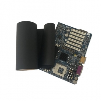
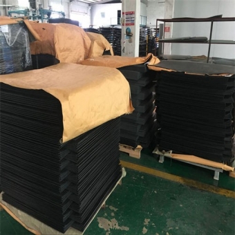
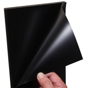
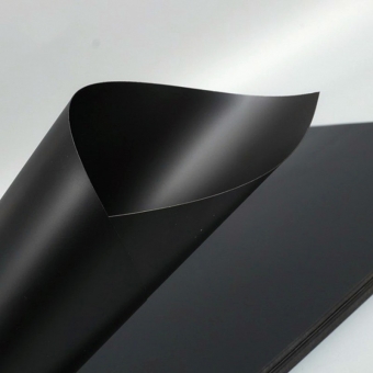
El proceso de termoformado somete a las láminas de HIPS a un calor intenso y a un estiramiento mecánico. Durante la fase de calentamiento, la lámina de plástico debe ablandarse uniformemente para permitir una replicación precisa del molde. Sin embargo, si el polímero tiene una distribución de peso molecular inestable, su ventana de temperatura de termoformado se vuelve demasiado estrecha. Esta inestabilidad hace que la lámina se combe prematuramente o se adelgace de manera desigual durante el estirado al vacío. En casos graves, el estiramiento extremo puede causar reventones de pared, donde el plástico se rompe en los huecos profundos. Para evitar estos fallos, los procesadores suelen utilizar láminas más gruesas de lo necesario, lo que aumenta los costos de material. Por el contrario, las formulaciones avanzadas de HIPS personalizadas ofrecen una ventana de temperatura de termoformado amplia y estable. Esta estabilidad térmica permite a los ingenieros de envasado reducir de forma segura el espesor de la materia prima. Por ejemplo, pueden pasar de una lámina de 1,2 milímetros a una solución de láminas de plástico HIPS de color negro de 1 mm de espesor sin sacrificar el rendimiento protector. El material optimizado fluye uniformemente hacia las cavidades del molde, manteniendo un espesor de pared constante incluso en diseños de embutición profunda. Esta distribución uniforme del material garantiza que las bandejas terminadas protejan los componentes electrónicos pesados o afilados. Al reducir el consumo de materia prima, los envasadores de productos electrónicos pueden reducir directamente sus costos de producción. Además, el espesor de pared uniforme mejora la apilabilidad de las bandejas terminadas. Cuando los huecos son idénticos, las bandejas encajan perfectamente sin pegarse.
En las operaciones típicas de termoformado, el desperdicio de esqueleto o los recortes representan un costo oculto masivo. Las láminas estándar a menudo resultan en más de un treinta por ciento de desperdicio de borde después de que se troquelan las piezas. Aunque algunas fábricas intentan reciclar este desperdicio, el reprocesamiento degrada el polímero y altera sus propiedades físicas. Por lo tanto, la forma más eficaz de reducir los costos es minimizar el desperdicio de recortes desde el principio. Los servicios personalizados OEM y ODM permiten a los envasadores de productos electrónicos pedir láminas en anchos de rollo adaptados que coincidan con sus diseños de molde específicos. Este dimensionamiento exacto elimina prácticamente el recorte de borde innecesario, lo que genera ahorros inmediatos de material. Además, los científicos de materiales pueden optimizar la contracción inducida por la orientación de la lámina de HIPS durante la extrusión. Al equilibrar la contracción tanto en la dirección de la máquina como en la dirección transversal, el material mantiene sus dimensiones durante el calentamiento. Esta estabilidad dimensional superior permite a los diseñadores de herramientas colocar las cavidades más cerca entre sí en el molde. En consecuencia, pueden maximizar el número de huecos por metro cuadrado de lámina de plástico. Reducir el espacio entre las piezas minimiza el desperdicio de esqueleto y aumenta el rendimiento de la producción. Además, las longitudes de rollo personalizadas permiten tiradas de producción continuas más largas con menos cambios de rollo. Menos cambios significan menos tiempo de inactividad de la máquina y una mayor eficacia general del equipo.
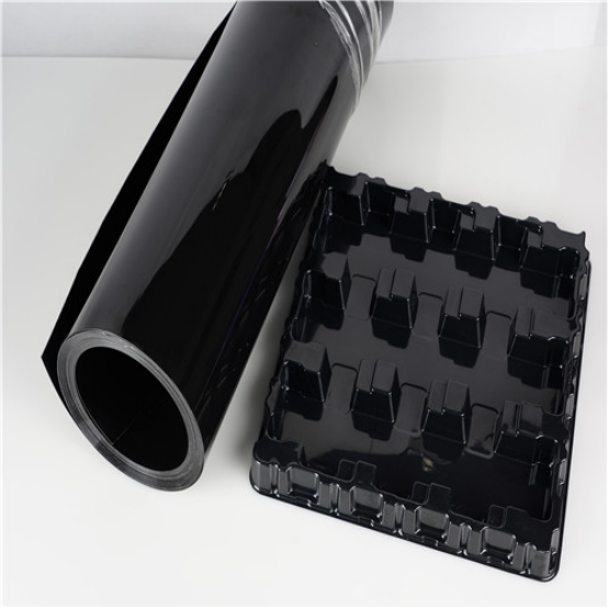
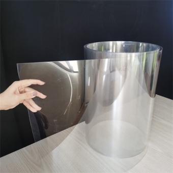
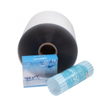
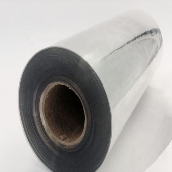
Lograr estas ventajas técnicas y de ahorro de costos requiere un socio de fabricación con una profunda experiencia en polímeros. En el competitivo mercado global de envasado de productos electrónicos, Fullstar (Xiamen Fullstar Imp.&Exp.Trading Co.,Ltd.) destaca como un recurso técnico de primer nivel. La empresa se especializa en el desarrollo de láminas de alto rendimiento a medida que optimizan los rendimientos de fabricación posteriores. Respaldado por una trayectoria de veinte años de excelencia en ingeniería, el proveedor global aprovecha un modelo operativo de doble base para servir a clientes internacionales. Sus instalaciones de investigación y desarrollo en China innovan continuamente en mezclas de polímeros, mientras que sus avanzadas líneas de fabricación en Malasia garantizan una producción de gran volumen y rentable. Para satisfacer las diversas necesidades de los fabricantes de productos electrónicos, Fullstar ofrece una línea completa de productos de HIPS. Sus rollos de láminas de poliestireno de alto impacto para conformado al vacío están diseñados específicamente para una excelente estabilidad térmica y capacidad de estirado. Además, para entornos de sala blanca que requieren una higiene impecable, la empresa fabrica rollos de HIPS blanco de grado alimenticio especializados, lo que demuestra sus versátiles capacidades de composición. Al controlar las tolerancias de espesor de la lámina dentro de micras, Xiamen Fullstar Imp.&Exp.Trading Co.,Ltd. evita atascos de alimentación y errores mecánicos en líneas automatizadas. El equipo técnico especializado trabaja en estrecha colaboración con los ingenieros de embalaje para ajustar la rigidez, la resistencia al impacto y las especificaciones de color. Este enfoque colaborativo permite a los clientes globales lograr importantes ahorros de costes sin comprometer la seguridad de sus delicados componentes electrónicos. Elegir un proveedor certificado y con gran experiencia minimiza los riesgos técnicos del desarrollo a medida. A través de la innovación continua de materiales, el proveedor global sigue siendo un socio de confianza en la cadena de suministro de productos electrónicos.
Descubra la gama completa de productos técnicos de HIPS y las opciones personalizables en el sitio web corporativo oficial:https://www.fullstarxm.com/.
XIAMEN FULLSTAR IMP.& EXP. TRADING CO.,LTD.


 red ipv6 compatible
 escanear a wechat :

 fullstar@xmfullstar.com
 es
es en
en ru
ru