In the production and packaging of semiconductors, PCBs, and IC chips, issues such as electrostatic discharge (ESD), dust contamination, and burrs during die-cutting have long plagued production yields. Conventional paper materials are prone to shedding dust and particles, while some plastic sheets are difficult to manage regarding static electricity and are liable to fray or tear during processing—leading to component scratches, ESD-induced breakdown, and hidden costs.
With over 20 years of experience in plastics manufacturing, we specialize in HIPS, APET, and PP sheets, as well as electronic-grade PP synthetic paper. Our products are engineered to solve material-related challenges in the isolation and protection of electronic components, combining three core performance attributes—anti-static properties, dust-free cleanliness, and excellent die-cutting capabilities—to perfectly suit precision electronics manufacturing environments.
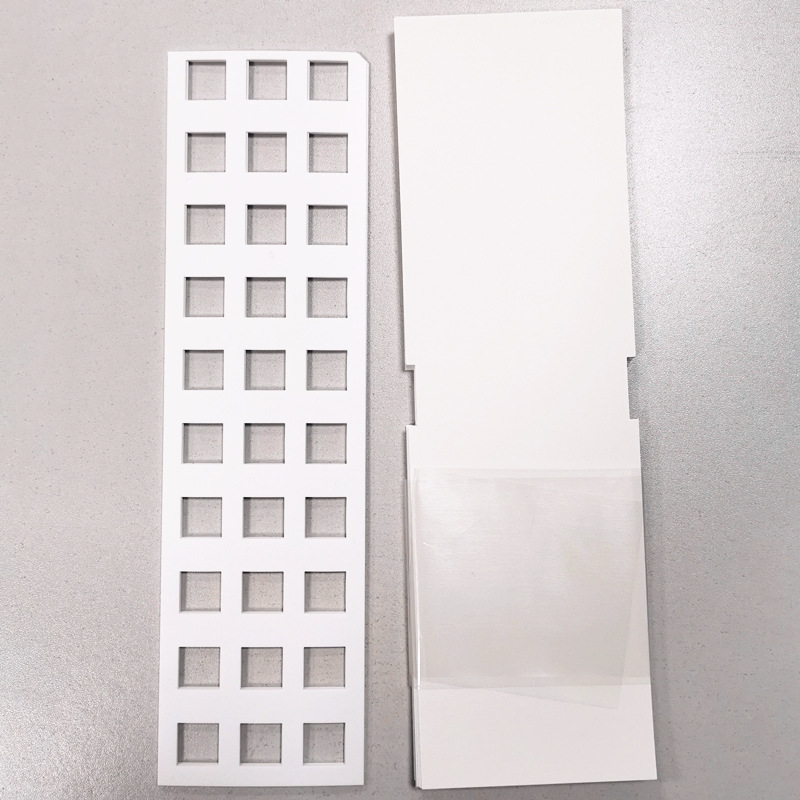
1. Core Advantages of PP Synthetic Paper: Directly Addressing Industry Pain Points
(1)Anti-static Properties: Preventing ESD Damage
Effectively dissipates static electricity and reduces charge accumulation, preventing ESD-induced breakdown in sensitive ICs, chips, and semiconductor devices. This ensures component integrity during assembly, handling, and transport, while minimizing the risk of scrap caused by static electricity.
(2)Dust-free Cleanliness: Eliminating Dust Contamination
Features a dense, smooth surface that resists dust particle adhesion and does not shed powder or debris like conventional paper. Ideal for cleanroom production lines, it prevents microscopic dust from contaminating precision electronic components, eliminates the need for repetitive cleaning, and maintains production line cleanliness.
(3) Excellent Die-cutting Performance: High Efficiency and Material Savings
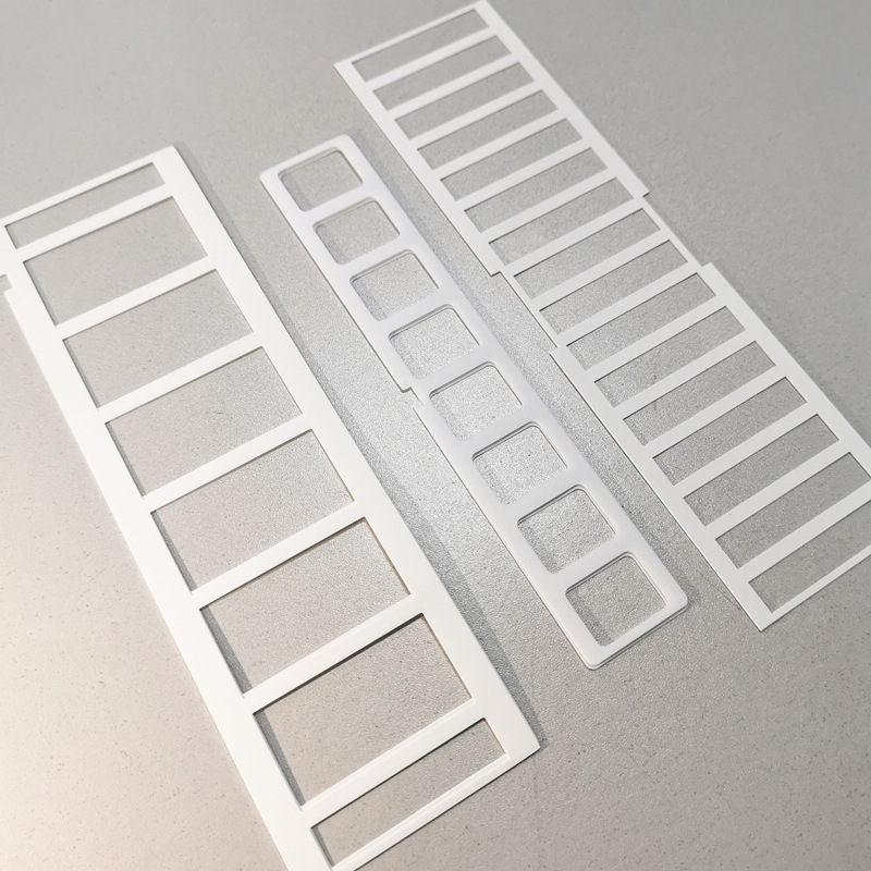
Offers uniform thickness and a stable material structure, ensuring clean, crisp die-cut edges without fraying or tearing. It is easily processed into various electronic isolation spacers and strips, is compatible with automated die-cutting lines, boosts processing efficiency, and reduces material costs. Key Application Scenarios
- Cushioning, protection, and isolation for ICs, chips, and semiconductor devices
- Specialized isolation lead frame spacer.
- Scratch-resistant and wear-resistant separator sheets for electronic packaging
2.Key Physical Properties
Thickness range: 0.1–1.0 mm (tolerance ±4%); Density: 1.2 g/cm³; Whiteness: 85; Surface resistance: 9×10¹² Ω/cm². The material exhibits stable tensile strength and elongation properties; metrics are tested in accordance with GB and ASTM standards. Maximum roll width is 750 mm; custom specifications are available upon request.
> Note: The parameters above are reference values based on laboratory testing. Customers are advised to verify the material against their specific operating conditions upon receipt.
3. Storage and Transport Guidelines
Avoid direct sunlight during storage and transport; prevent impact and exposure to rain during handling. Use within six months of production to ensure material performance stability.
We also supply various plastic sheets, including HIPS and APET, offering one-stop material selection solutions for electronic packaging and die-cut spacers. If you are looking for a reliable base material for anti-static, clean-room compatible spacers, please contact us for samples .
XIAMEN FULLSTAR IMP.& EXP. TRADING CO.,LTD.


 red ipv6 compatible
 escanear a wechat :

 fullstar@xmfullstar.com
 es
es en
en ru
ru